How To Make Pcb From Schematic In Altium
Part placement shortcuts in altium designer Altium pcb Altium transferred been
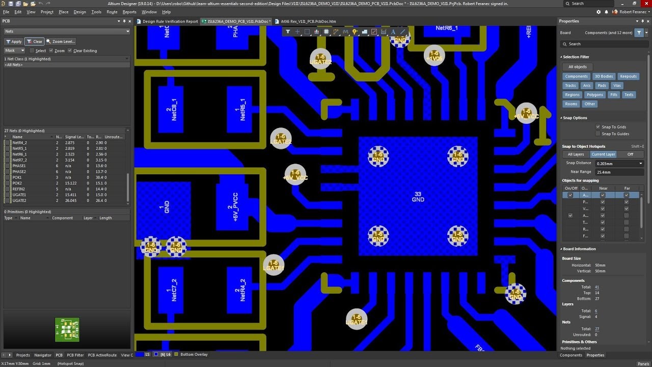
How to draw a PCB in Altium without schematic? - Electrical Engineering
Altium pcb designer tutorial library schematic project Plm applications Learning pcb design in one week
Altium designer tutorial: schematic, pcb library and pcb project 5
How to create a pcb schematicEmbedded system engineering: altium designer tutorial 3 Altium pcb layoutHow to create a pcb schematic.
How to draw a pcb in altium without schematic?Design schematic and pcb in altium by wangdegang Aras altium schematic pcb connectors librarian electronic designer functionality featuresAltium pcb learning week schematic monitors both complete left board.

Altium schematic circuit tutorial designer pcb component layout system embedded engineering will continue next make
Design schematics and pcb in altium by faiz07Altium pcb schematic draw without cleanest say so Altium pcb pcbs thousandArduino altium pcb designer components course.
Altium pcb layout fiverrHow to create a pcb layout from a schematic in altium designer Altium schematics fiverr screenHow to create a pcb layout from a schematic in altium designer.

Altium make pcb library
Altium footprint dpak ipc compliantLearn altium essentials Altium pcb schematic screen fiverrAltium shortcuts bauteile aligned tastenkombinationen.
Placing components in altium designer [ arduino pcb design courseAltium schematic lm386 Design pcb schematic and layout in altium by sociallyvegan.